Product Overview
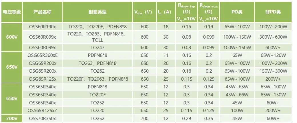
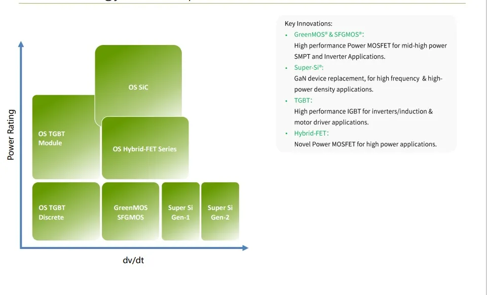
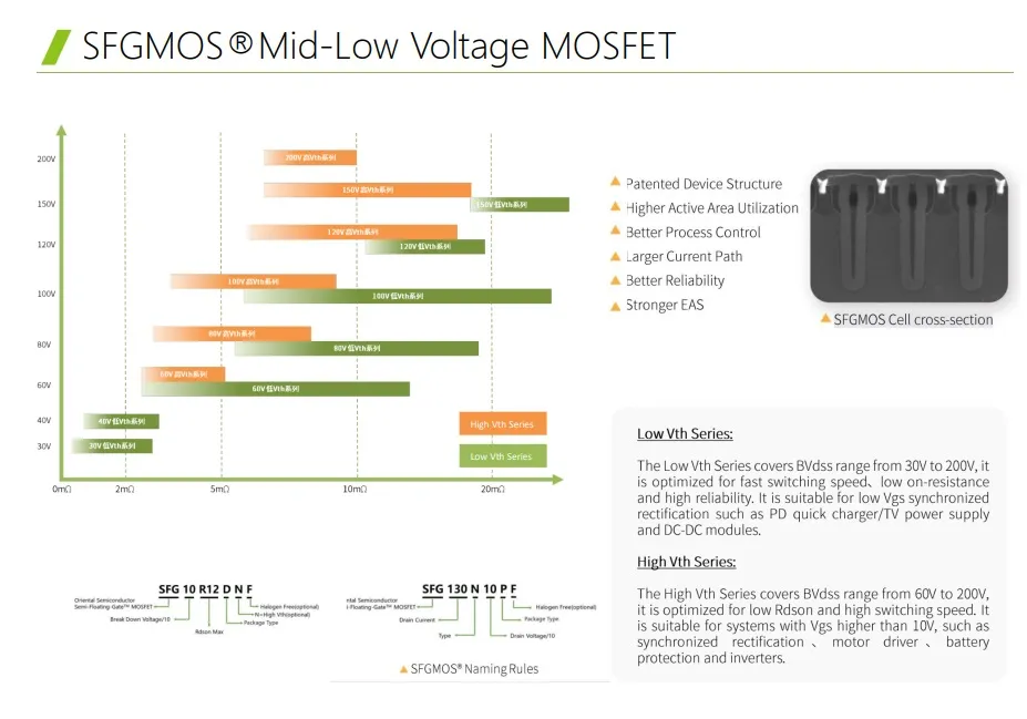
The GreenMOS® high voltage MOSFET utilizes charge balance technology to achieve outstanding low on-resistance and lower gate charge. It is engineered to minimize conduction loss, provide superior switching performance and robust avalanche capability.
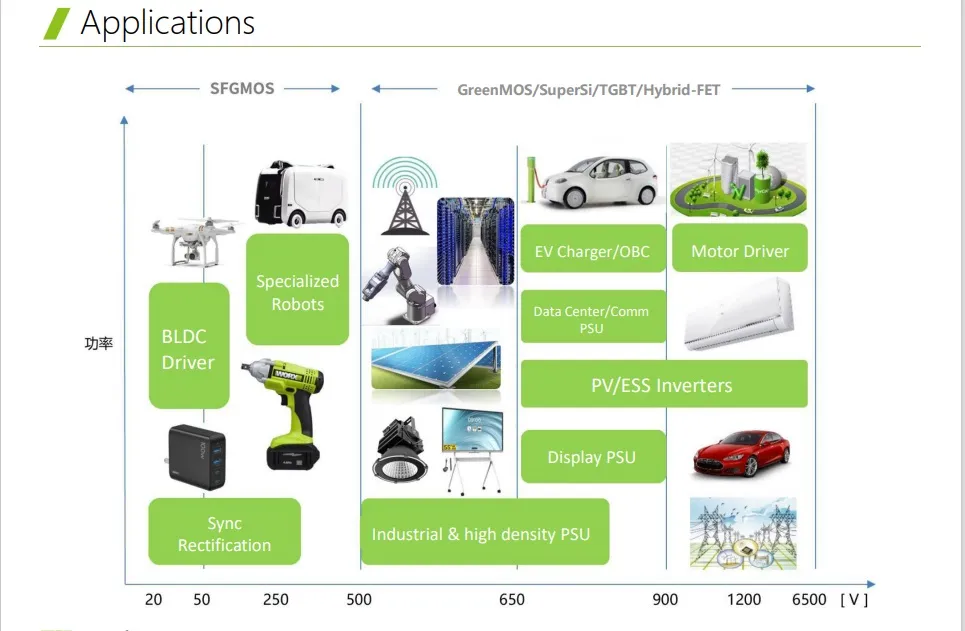
The GreenMOS® SuperSi series is based on unique device design to achieve extremely fast switching characteristics. It is the perfect replacement for the Gallium Nitride (GaN) device in high frequency operations with better ruggedness and cost. It is targeted to meet the most aggressive efficiency standards of power supply systems by pushing both performance and power density to extreme limits.
Frequently Asked Questions
What makes the OSS65R340DF a good alternative to GaN devices?
The SuperSi series offers extremely fast switching characteristics similar to Gallium Nitride (GaN) but with superior ruggedness and a significantly lower cost, making it ideal for high-frequency operations.
What is the maximum voltage rating for this MOSFET?
The OSS65R340DF has a drain-source breakdown voltage (BVSS) of 650V at room temperature, which reaches a minimum of 700V at 150°C.
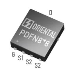
What are the primary applications for the TO252 package model?
It is specifically designed for PD chargers, large screen displays, telecom power systems, and high-density server power supplies.
How does the charge balance technology benefit the performance?
This technology allows for an outstandingly low on-resistance (RDS(ON)) and lower gate charge, which directly translates to minimized conduction losses and improved efficiency.
Is this component compliant with international standards?
Yes, the product is engineered to meet aggressive efficiency standards for modern power supply systems while maintaining robust avalanche capability and thermal stability.
What is the thermal resistance of the OSS65R340DF?
The junction-to-case thermal resistance (RθJC) is 1.5 °C/W, ensuring efficient heat dissipation during high-power operations.