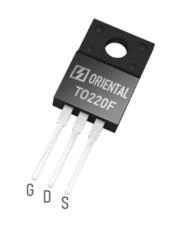
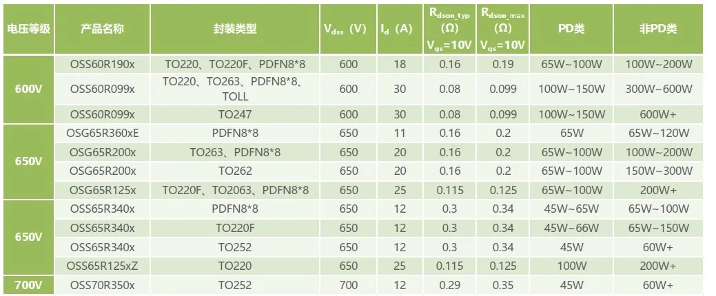
Model NO.OSS65R340DF TO252
IndustriesLED Lighting
Transport PackageAir
OriginChina
HS Code854129000
Capacity20kkkk/Monthly
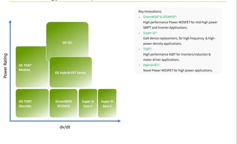
The GreenMOS® high voltage MOSFET utilizes charge balance technology to achieve outstanding low on-resistance and lower gate charge. It is engineered to minimize conduction loss, provide superior switching performance and robust avalanche capability.
The GreenMOS® SuperSi series is based on unique device design to achieve extremely fast switching characteristics. It is the perfect replacement for the Gallium Nitride (GaN) device in high frequency operations with better ruggedness and cost. It is targeted to meet the most aggressive efficiency standards of power supply systems by pushing both performance and power density to extreme limits.
- Low RDS(ON) & FOM
- Extremely low switching loss
- Excellent stability and uniformity
- Easy to design in
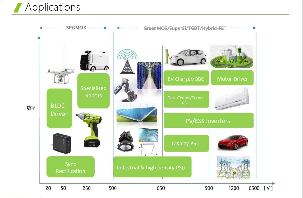
- PD charger
- Large screen display
- Telecom power
- Server power
Key Performance Parameters
| Parameter | Value | Unit |
|---|
| VDS, min @ Tj(max) | 700 | V |
| ID, pulse | 36 | A |
| RDS(ON), max @ VGS=10V | 340 | mΩ |
| Qg | 9.6 | nC |
Absolute Maximum Ratings (Tj=25°C)
| Parameter | Symbol | Value | Unit |
|---|
| Drain-source voltage | VDS | 650 | V |
| Gate-source voltage | VGS | ±30 | V |
| Continuous drain current, TC=25 °C | ID | 12 | A |
| Continuous drain current, TC=100 °C | ID | 7.6 | A |
| Pulsed drain current | ID, pulse | 36 | A |
| Power dissipation, TC=25 °C | PD | 83 | W |
| Single pulsed avalanche energy | EAS | 200 | mJ |
| Operation and storage temperature | Tstg, Tj | -55 to 150 | °C |
Electrical Characteristics
| Parameter | Symbol | Min. | Typ. | Max. | Unit |
|---|
| Drain-source breakdown voltage | BVDSS | 650 | - | - | V |
| Gate threshold voltage | VGS(th) | 2.9 | - | 3.9 | V |
| Drain-source on-state resistance | RDS(ON) | - | 0.30 | 0.34 | Ω |
| Input capacitance | Ciss | - | 443.5 | - | pF |
| Total gate charge | Qg | - | 9.6 | - | nC |
| Diode forward voltage | VSD | - | - | 1.3 | V |
Technical Notes:
1) Calculated continuous current based on maximum allowable junction temperature.
2) Repetitive rating; pulse width limited by max. junction temperature.
3) Pd is based on max. junction temperature, using junction-case thermal resistance.
4) RθJA measured with device mounted on 1 in² FR-4 board with 2oz. Copper.
5) VDD=100 V, VGS=10 V, L=60 mH, starting Tj=25 °C.
Frequently Asked Questions
What makes the GreenMOS® SuperSi series unique?
It uses a proprietary device design to achieve extremely fast switching characteristics, making it an ideal, cost-effective replacement for Gallium Nitride (GaN) devices in high-frequency applications.
What are the main advantages of charge balance technology in this MOSFET?
Charge balance technology allows the OSS65R340DF to achieve outstandingly low on-resistance (RDS(ON)) and lower gate charge, which significantly reduces conduction and switching losses.
What is the maximum voltage rating for the OSS65R340DF?
The device has a minimum drain-source breakdown voltage (BVDSS) of 650V at room temperature, reaching up to 700V at a junction temperature of 150°C.
In which applications is this MOSFET typically used?
It is specifically designed for high-efficiency power systems including PD chargers, large screen displays, telecom power supplies, and server power units.
What is the avalanche capability of this model?
The OSS65R340DF features robust avalanche capability with a single pulsed avalanche energy (EAS) rating of 200mJ, ensuring reliability under extreme stress conditions.
What are the thermal resistance characteristics?
The maximum thermal resistance from junction to case (RθJC) is 1.5 °C/W, allowing for efficient heat dissipation in demanding power density environments.