

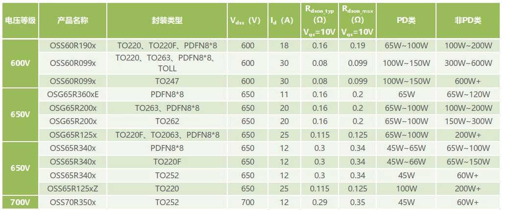

1 / 5
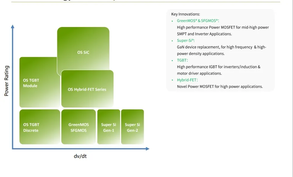
The GreenMOS® high voltage MOSFET utilizes charge balance technology to achieve outstanding low on-resistance and lower gate charge. It is engineered to minimize conduction loss, provide superior switching performance and robust avalanche capability.
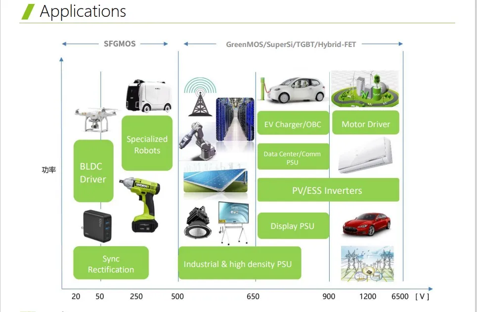
The GreenMOS® SuperSi series is based on unique device design to achieve extremely fast switching characteristics. It is the perfect replacement for Gallium Nitride (GaN) devices in high frequency operations with better ruggedness and cost efficiency. It meets aggressive efficiency standards by pushing performance and power density to extreme limits.
| Parameter | Value | Unit |
|---|---|---|
| VDS, min @ Tj(max) | 700 | V |
| ID, pulse | 36 | A |
| RDS(ON), max @ VGS=10V | 340 | mΩ |
| Qg | 9.6 | nC |
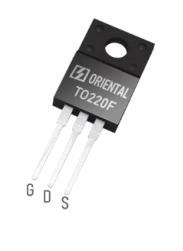
| Parameter | Symbol | Value | Unit |
|---|---|---|---|
| Drain-source voltage | VDS | 650 | V |
| Gate-source voltage | VGS | ±30 | V |
| Continuous drain current (TC=25 °C) | ID | 12 | A |
| Continuous drain current (TC=100 °C) | ID | 7.6 | A |
| Pulsed drain current | ID, pulse | 36 | A |
| Power dissipation (TC=25 °C) | PD | 83 | W |
| Single pulsed avalanche energy | EAS | 200 | mJ |
| Operation and storage temperature | Tstg, Tj | -55 to 150 | °C |


Notes: 1. Continuous current based on max junction temperature. 2. Pulse width limited by max junction temperature. 3. Pd based on junction-to-case thermal resistance. 4. EAS tested at VDD=100V, L=60mH.