


1 / 5
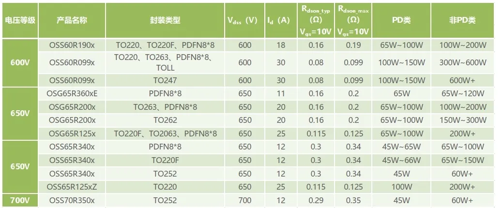
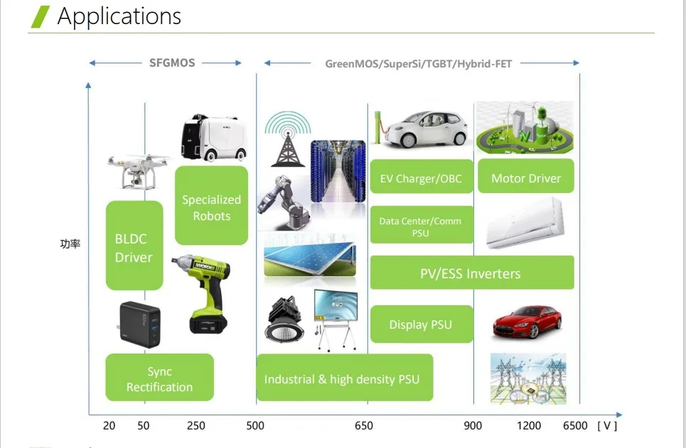
The GreenMOS® high voltage MOSFET utilizes charge balance technology to achieve outstanding low on-resistance and lower gate charge. It is engineered to minimize conduction loss, provide superior switching performance and robust avalanche capability.
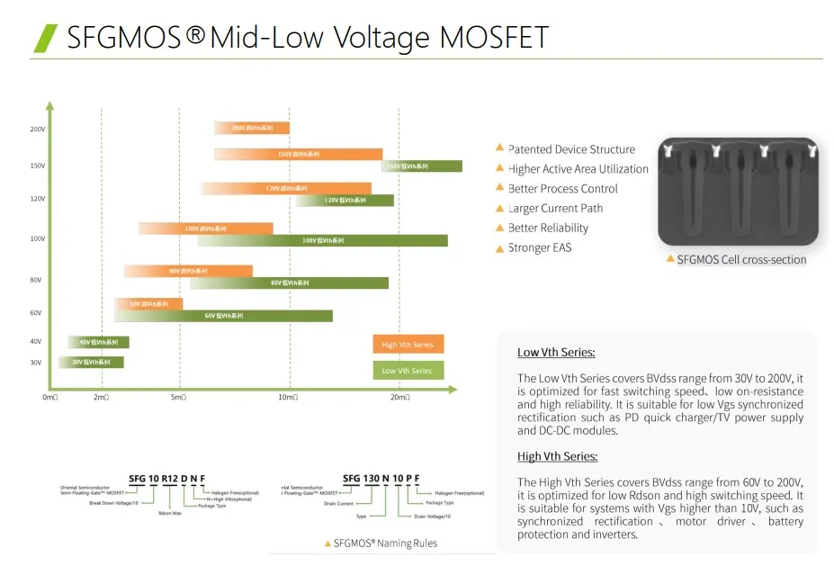
The GreenMOS® SuperSi series is based on unique device design to achieve extremely fast switching characteristics. It is the perfect replacement for Gallium Nitride (GaN) devices in high frequency operations with better ruggedness and cost. It is targeted to meet the most aggressive efficiency standards of power supply systems by pushing both performance and power density to extreme limits.
| Parameter | Value | Unit |
|---|---|---|
| VDS, min @ Tj(max) | 700 | V |
| ID, pulse | 36 | A |
| RDS(ON), max @ VGS=10V | 340 | mΩ |
| Qg | 9.6 | nC |
| Product Name | Package | Marking |
|---|---|---|
| OSS65R340JF | PDFN8×8 | OSS65R340J |
| Parameter | Symbol | Value | Unit |
|---|---|---|---|
| Drain-source voltage | VDS | 650 | V |
| Gate-source voltage | VGS | ±30 | V |
| Continuous drain current, TC=25 °C | ID | 12 | A |
| Continuous drain current, TC=100 °C | ID | 7.6 | A |
| Pulsed drain current | ID, pulse | 36 | A |
| Power dissipation, TC=25 °C | PD | 83 | W |
| Single pulsed avalanche energy | EAS | 200 | mJ |
| Operation and storage temperature | Tstg, Tj | -55 to 150 | °C |
| Parameter | Symbol | Min. | Typ. | Max. | Unit |
|---|---|---|---|---|---|
| Drain-source breakdown voltage | BVDSS | 650 | - | - | V |
| Gate threshold voltage | VGS(th) | 2.9 | - | 3.9 | V |
| Drain-source on-state resistance | RDS(ON) | - | 0.30 | 0.34 | Ω |
| Gate-source leakage current | IGSS | - | - | 100 | nA |
| Drain-source leakage current | IDSS | - | - | 1 | μA |
| Parameter | Symbol | Typ. | Unit | Test Condition |
|---|---|---|---|---|
| Input capacitance | Ciss | 443.5 | pF | VGS=0V, VDS=50V, f=100KHz |
| Output capacitance | Coss | 59.6 | pF | |
| Reverse transfer capacitance | Crss | 1.7 | pF | |
| Turn-on delay time | td(on) | 22.4 | ns | VGS=10V, VDS=400V, ID=6A |
| Turn-off delay time | td(off) | 40.3 | ns |
| Parameter | Symbol | Typ. | Max. | Unit |
|---|---|---|---|---|
| Diode forward voltage | VSD | - | 1.3 | V |
| Reverse recovery time | trr | 236.5 | - | ns |
| Reverse recovery charge | Qrr | 2.2 | - | μC |
| Peak reverse recovery current | Irrm | 19.1 | - | A |