


1 / 5
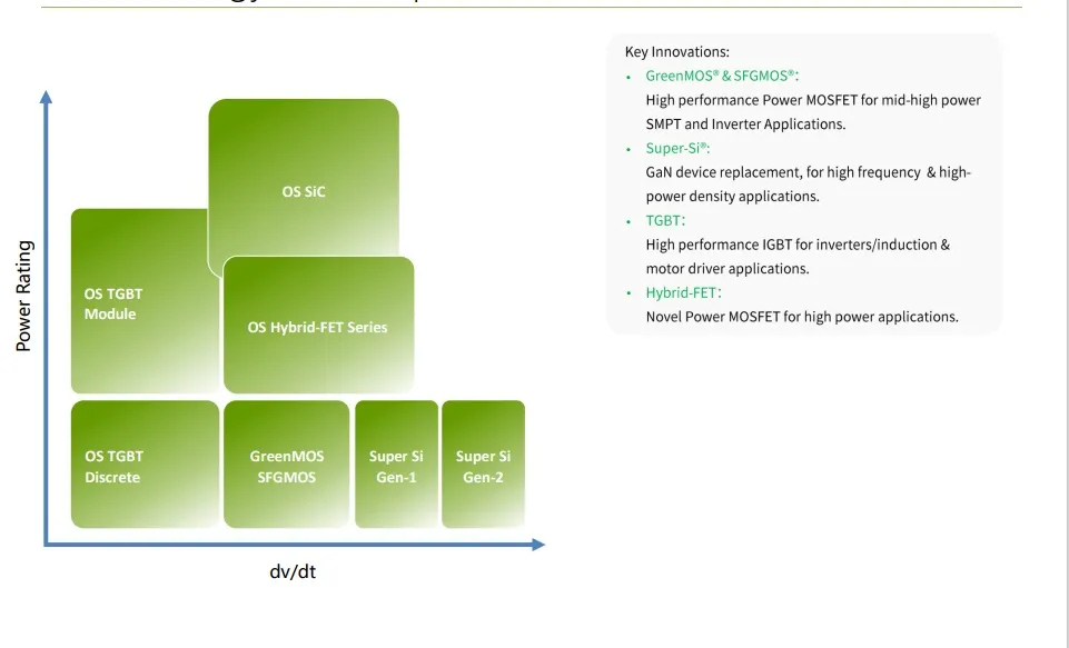
The GreenMOS® high voltage MOSFET utilizes charge balance technology to achieve outstanding low on-resistance and lower gate charge. It is engineered to minimize conduction loss, provide superior switching performance and robust avalanche capability.
The SuperSi series is based on unique device design to achieve extremely fast switching characteristics. It is the perfect replacement for the Gallium Nitride (GaN) device in high frequency operations with better ruggedness and cost. It is targeted to meet the most aggressive efficiency standards of power supply systems by pushing both performance and power density to extreme limits.

| Parameter | Symbol | Value | Unit | Test Condition |
|---|---|---|---|---|
| Drain-source voltage | VDS | 650 | V | - |
| Gate-source voltage | VGS | ±30 | V | - |
| Continuous drain current | ID | 12 | A | TC=25 °C |
| Pulsed drain current | ID, pulse | 36 | A | TC=25 °C |
| Power dissipation | PD | 83 | W | TC=25 °C |
| Drain-source breakdown voltage | BVDSS | 650 / 700 | V | VGS=0 V, ID=250 μA |
| Gate threshold voltage | VGS(th) | 2.9 - 3.9 | V | VDS=VGS, ID=250 μA |
| Drain-source on-state resistance | RDS(ON) | 0.30 - 0.34 | Ω | VGS=10 V, ID=6 A |
| Parameter | Symbol | Typ. Value | Unit |
|---|---|---|---|
| Input capacitance | Ciss | 443.5 | pF |
| Output capacitance | Coss | 59.6 | pF |
| Reverse transfer capacitance | Crss | 1.7 | pF |
| Total gate charge | Qg | 9.6 | nC |
| Gate-source charge | Qgs | 2.2 | nC |
| Gate-drain charge | Qgd | 4.5 | nC |


A: The SuperSi series offers extremely fast switching characteristics and is designed as a cost-effective, more rugged alternative to Gallium Nitride (GaN) devices in high-frequency applications.
A: It has a Drain-source voltage rating of 650V, which can reach 700V at maximum junction temperatures.
A: It is specifically designed for high-efficiency systems such as PD chargers, telecom power, server power, and large screen displays.
A: It allows the device to achieve outstandingly low on-resistance (RDS(ON)) and lower gate charge, effectively minimizing conduction and switching losses.
A: This model uses the PDFN8x8 package, which is optimized for power density and thermal performance.
A: The GreenMOS® technology provides a robust avalanche capability, with a single pulsed avalanche energy (EAS) rating of 200 mJ.